
This application note discusses the input and output characteristics of the MM74HC high-speed CMOS logic family, as well as how these characteristics are affected by various parameters such as power supply voltage and temperature. Also, for those users who have been designing with metal-gate CMOS and TTL logic, this application note compares the notable differences and features of high-speed CMOS to those logic families.
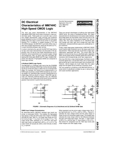
The document introduces the MM74HC high‑speed CMOS logic family, describing its buffered architecture and the advantages of buffering for noise immunity and output drive. It compares the family to CD4000, MM74C, and low‑power Schottky TTL families, and notes the TTL‑compatible MM74HCT sub‑family.
Key electrical specifications are provided, including input voltage thresholds, output voltage levels, supply voltage range (2–6 V), typical output drive currents (4 mA standard, 6 mA bus driver) and absolute maximum ratings such as VCC limits and diode currents. The note also covers input capacitance, quiescent current, and protection against electrostatic discharge.
| Input high voltage (VIH) at VCC=5 V | 3.5 V |
|---|---|
| Input low voltage (VIL) at VCC=5 V | 1.0 V |
| Input high voltage (VIH) over supply range | 0.7 × VCC |
| Input low voltage (VIL) over supply range | 0.2 × VCC |
| Supply voltage range | 2 V – 6 V |
| Standard output current rating | ±25 mA per pin |
| Bus driver output current rating | ±35 mA per pin |
| Maximum VCC rating | 7 V |
MM74HC devices are specified to operate from 2 V to 6 V.
At VCC = 5 V, the input high threshold (VIH) is 3.5 V and the input low threshold (VIL) is 1.0 V.
The absolute maximum rating for a standard output pin is ±25 mA.