
74VHC175 is an advanced high-speed CMOS device fabricated with silicon gate CMOS technology. It achieves the high-speed operation similar to equivalent Bipolar Schottky TTL while maintaining the CMOS low power dissipation.
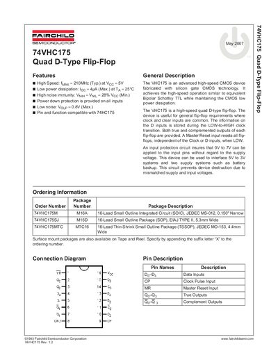
The 74VHC175 is a high‑speed CMOS quad D‑type flip‑flop that stores data on the rising edge of a common clock input and provides both true and complemented outputs. It features low power consumption, input over‑voltage protection up to 7 V, and is pin‑compatible with the 74HC175 family.
Electrical specifications include a typical maximum clock frequency of 210 MHz at 5 V, supply voltage range of 2.0 V to 5.5 V, and operation from –40 °C to +85 °C. The device is offered in 16‑lead SOIC, SOP, and TSSOP packages with detailed mechanical dimensions provided.
| Supply voltage range | 2.0 V to 5.5 V |
|---|---|
| Input voltage range (over‑voltage protection) | OV to 5.5 V |
| Operating temperature | -40 °C to +85 °C |
| Storage temperature | -65 °C to +150 °C |
It works with a supply voltage of 2.0 V to 5.5 V and input voltage from OV to 5.5 V.
Yes, the inputs can tolerate up to 7 V regardless of the supply voltage.