
This application note compares Fairchild Semiconductor's logic solutions for buffered (or registered) DIMMs to other competitive solutions. Proper selection of the logic devices to register and redrive heavily loaded address and control signal paths requires careful consideration of device parameters and can result in a SDRAM DIMM design that uses the fewest components and provides reliable circuit performance.
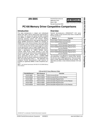
This application note provides functional and AC performance comparisons between Fairchild Semiconductor's VCX family (e.g., 74VCX16835, 74VCX162835) and comparable ALVC devices for PC100 registered DIMM applications. It includes device tables, connection diagrams, and detailed timing specifications.
The document also contains a life‑support policy disclaimer and concludes that Fairchild's solutions offer comparable or better performance than competing parts, helping designers achieve high signal integrity in DIMM designs.
| CLK Input Voltage (VCX) | 3.30 V – 6.00 V |
|---|---|
| Maximum Clock Frequency | 150 MHz |
| Setup Time (VCX) | 0.7 ns |
The CLK input voltage must be between 3.30 V and 6.00 V.
Yes, the VCX and ALVC devices are pin and functionally equivalent.
The maximum allowable propagation delay is 300 ps.