
Datasheet for the FDG6316P P-Channel MOSFET, optimized for battery power management with low RDS(on) and SC70-6 package.
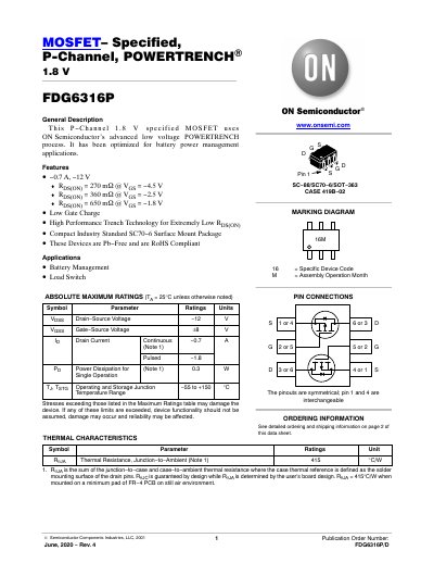
This datasheet details the FDG6316P P-Channel MOSFET, designed for battery power management using ON Semiconductor’s POWERTRENCH process. It includes electrical, thermal, and mechanical specifications. The device is available in a compact SC70-6 surface mount package and is Pb-free and RoHS compliant. Key features include low gate charge, high performance trench technology, and specified RDS(on) values at various gate-source voltages.
| RDS(on) at VGS = -4.5V | 270 mΩ |
|---|---|
| RDS(on) at VGS = -2.5V | 360 mΩ |
| RDS(on) at VGS = -1.8V | 650 mΩ |
| Gate Threshold Voltage | −0.4 to −1.5 V |
| Drain-Source Voltage | −12 V |
| Drain Current | −0.7 A |
| Thermal Resistance | 415 °C/W |
The maximum drain-source voltage is −12 V.
The gate threshold voltage ranges from −0.4 V to −1.5 V.
The thermal resistance is 415 °C/W.