
The MC74VHC1G50 is an advanced high speed CMOS buffer fabricated with silicon gate CMOS technology. It achieves high speed operation similar to equivalent Bipolar Schottky TTL while maintaining CMOS low power dissipation. The internal circuit is composed of three stages, including a buffered output which provides high noise immunity and stable output. The MC74VHC1G50 input structure provides protection when voltages up to 7V are applied, regardless of the supply voltage. This allows the MC74VHC1G50 to be used to interface 5V circuits to 3V circuits.
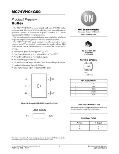
The MC74VHC1G50 is an advanced high‑speed CMOS buffer that provides a buffered output for high noise immunity and stable logic levels. It features input protection for voltages up to 7 V, allowing 5 V circuits to interface with 3 V circuits, and offers low power dissipation.
The datasheet lists maximum ratings, recommended operating conditions, and detailed DC and AC electrical characteristics, including propagation delay, input‑high/low thresholds, and output current capabilities. Ordering information, package dimensions, and tape/reel specifications are also provided.
| Propagation delay (tpp) | 3.5 ns typ |
|---|---|
| Supply voltage (VCC) | 2.0 – 5.5 V |
| Input high voltage (VIH) min | 2.0 V |
| Input low voltage (VIL) max | 0.5 V |
| Output current per pin (IOUT) | 25 mA max |
| Power dissipation (Pp) in still air | 200 mW |
| Package type | 5‑lead SOT‑353 (SC‑88A) |
The device can be powered from 2.0 V up to 5.5 V.
It is supplied in a 5‑lead SOT‑353 (SC‑88A) package.
The typical propagation delay is 3.5 ns at a 5 V supply.