
This application note provides hardware design guidelines for SPC560B4x/5x and SPC560C4x/5x, including requirements for power supply, reset control, clock management, boot mode setting, debug management, and I/O settings.
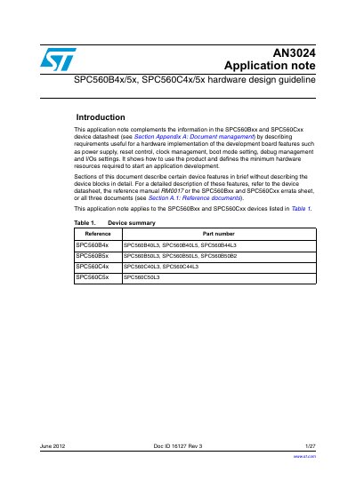
This application note complements the device datasheets for the SPC560Bxx and SPC560Cxx families by describing requirements for hardware implementation. It details how to use the product and defines the minimum hardware resources required to start application development, including power supply, reset control, clock management, boot mode setting, debug management, and I/O settings.
The document provides specific guidance on power supply schemes, current consumption, and layout recommendations. It also covers reset schemes, ADC performance optimization, external oscillator configurations (fast and slow), boot configuration methods, JTAG debugging, I/O characteristics, and EMC guidelines. A reference schematic is included to illustrate typical application designs.
| Operating voltage supply | 3.3 V or 5.0 V |
|---|---|
| Internal digital power | 1.2 V |
The device requires a 3.3 V or 5.0 V operating voltage supply for high voltage pins, with an internal regulator providing 1.2 V for digital power.
No, the device cannot be supplied with external 1.2 V; the on-chip regulator must always be used.
The inrush current is clamped at 400 mA and lasts for a maximum of 20 microseconds until stabilization capacitors are charged.