
This document explains the design and setup of the evaluation board for the AD1937 and AD1939.
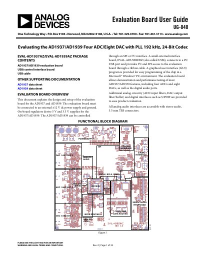
This document provides instructions for setting up and using the AD1937/AD1939 Evaluation Board. It details the package contents, functional block diagram, and hardware setup procedures including powering the board and configuring the master clock (MCLK). The guide explains how to operate the board in standalone mode or via SPI/I2C control using the USBi interface.
| ADC/DAC Count | Four ADCs and eight DACs |
|---|---|
| Power Supply Input | ±12 V dc |
| +12 V Current Draw | ~250 mA |
| -12 V Current Draw | ~100 mA |
| Control Interfaces | SPI or I2C |
The board requires an external ±12 V dc power supply and ground.
You can control them via SPI or I2C by connecting the port to the USBi interface.
A graphical user interface (GUI) program called Automated Register Window Builder is provided.