
Analog Devices AN-776 AD9981 Dual Chip Design Guideline

This application note describes how to use the AD9981 to design a dual chip solution to achieve UXGA resolutions.
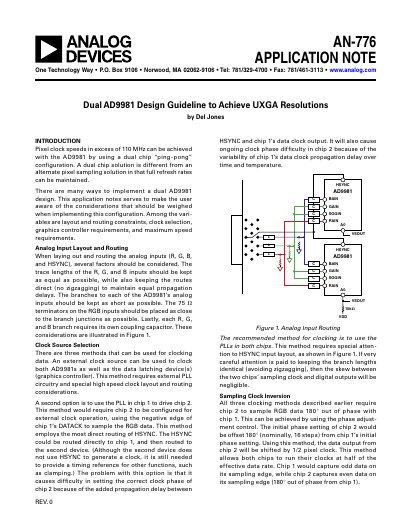

Analog Devices AN-776 AD9981 Dual Chip Design Guideline - cover page
Brand
Analog Devices
Category
Other Electronics
Document type
Application Note
Language
English
Pages
4
File format
PDF
File size
87 KB
Published
02 August, 2012
Updated
30 September, 2023
Model
AD9981
MD5 checksum
166D1F82B6CC8D7F25429F5A10D24BFA

About this manual

This application note discusses the implementation of a dual AD9981 design to achieve pixel clock speeds in excess of 110 MHz while maintaining full refresh rates. It details considerations for analog input layout and routing, including trace length matching and terminator placement. The document also covers clock source selection methods, specifically comparing external clocks, chip-to-chip driving, and the recommended dual PLL approach.

What's inside

  • Introduction
  • Analog Input Layout and Routing
  • Clock Source Selection
  • Sampling Clock Inversion
  • Clock Phase Adjustment
  • Interpart Difference Adjustments
  • Device Addressing
  • Data Mode Selection
  • Reference Designs

Frequently asked questions

What pixel clock speeds can be achieved with a dual AD9981 configuration?

Pixel clock speeds in excess of 110 MHz can be achieved with the AD9981 by using a dual chip configuration.

How many data output traces are required for a dual AD9981 design?

Single-channel mode requires 60 data output traces and requires a graphics controller that has 60 data input lines.

What is the maximum operating speed when data switching is used?

Data switching limits the maximum operating speed to 220 MHz.

Download PDF (87 KB)

More Analog Devices Manuals


View all Analog Devices manuals →