
This is a Hynix 4 Banks x 1M x 32Bit Synchronous DRAM, which has 134,217,728-bit CMOS Synchronous DRAM, ideal for memory applications that require wide data I/O and high bandwidth.
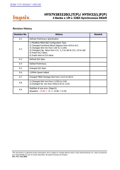
This document is a general product description for the Hynix HY57V283220(L)T(P) / HY5V22(L)F(P) Synchronous DRAM. The device is a 134,217,728-bit CMOS SDRAM organized as 4 banks of 1,048,576 x 32, designed for memory applications requiring wide data I/O and high bandwidth.
| Organization | 4 Banks x 1M x 32 |
|---|---|
| Capacity | 134,217,728 bits |
| Power Supply | 3.3V |
| Interface | LVTTL |
| Refresh Cycles | 4096 / 64ms |
The device is organized as 4 banks of 1,048,576 x 32.
Yes, all device pins are compatible with LVTTL interface.
The device uses a JEDEC standard 3.3V power supply.