
This document introduces a single-supply-powered flash chip that features high performance, ultra-low power consumption, top and bottom boot block versions, secured sector, and sector protection.
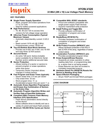
The HY29LV320 is a 32 Mbit CMOS Flash memory organized as 2M words, available in 48-pin TSOP and 63-ball FBGA packages. It operates on a single 3 volt VCC supply ranging from 2.7 to 3.6 volts, eliminating the need for a higher voltage power supply for programming and erasing.
The device features sector erase architecture with top and bottom boot block versions (HY29LV320B and HY29LV320T). It includes hardware write protection, an accelerated program function, and automatic sleep/standby modes to reduce power consumption. The memory is compliant with JEDEC standards and the Common Flash Memory Interface (CFI) specification.
| Capacity | 32 Mbit (2M x 16) |
|---|---|
| Operating Voltage | 2.7 to 3.6 volts |
| Access Time | 70 ns (typical) |
| Standby Current | 5.0 µA (max) |
| Read Current | 16 mA (max at 5 MHz) |
| Package Types | 48-pin TSOP and 63-ball FBGA |
No, it operates with a single 3 volt VCC supply. Internally generated and regulated voltages are provided for program and erase operations.
The typical sector erase time is 0.5 seconds per sector.