
This is a product description document that introduces Hynix Semiconductor's series of 200pin unbuffered DDR2 SODIMMs based on 512Mb 1st ver. DDR2 SDRAM. The series features a high-performance 8-byte interface in an industry-standard form factor, suitable for easy interchange and addition. The document also provides detailed information on different capacities and materials.
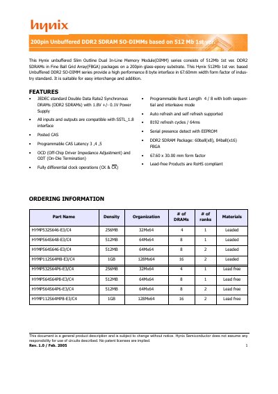
This document describes the Hynix 200pin Unbuffered DDR2 SDRAM SO-DIMM series based on 512Mb 1st generation DDR2 SDRAMs in FBGA packages. The modules utilize a 67.60mm width form factor and provide an 8-byte interface suitable for easy interchange and addition in industrial standard applications.
Key features include JEDEC standard Double Data Rate 2 Synchronous DRAMs with 1.8V power supply, SSTL_1.8 compatible inputs/outputs, programmable CAS latency (3, 4, or 5), and fully differential clock operations. The datasheet details pin descriptions, functional block diagrams for various densities (256MB to 1GB), speed grades (DDR2-400 and DDR2-533), and ordering information.
| Power Supply Voltage | 1.8V +/- 0.1V |
|---|---|
| Interface Standard | SSTL_1.8 |
| CAS Latency Options | 3, 4, or 5 |
| Form Factor Width | 67.60mm |
| Package Type | FBGA (60ball or 84ball) |
The modules operate with a 1.8V +/- 0.1V Power Supply.
The modules support programmable CAS Latency of 3, 4, or 5.
The module has a standard industry form factor width of 67.60mm.