
This document is about Hynix HY5V26C(L/S)F 4 Banks x 2M x 16bits Synchronous DRAM, a CMOS Synchronous DRAM that is ideal for main memory applications that require large memory density and high bandwidth.
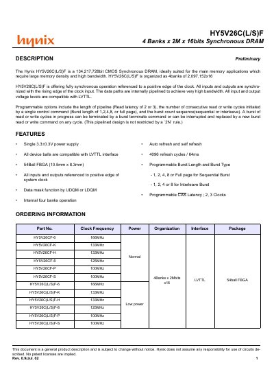
The Hynix HY5V26C(L/S)F is a 134,217,728-bit CMOS Synchronous DRAM designed for main memory applications requiring large density and high bandwidth. The device features fully synchronous operation referenced to the positive edge of the system clock with internally pipelined data paths.
| Memory Organization | 4 Banks x 2Mbits x 16 |
|---|---|
| Power Supply Voltage | 3.3 ±0.3V |
| Package Type | 54 Ball FBGA |
| Operating Temperature Range | 0 to 70 °C |
| Storage Temperature Range | -55 to 125 °C |
| Refresh Cycle Rate | 4096 cycles / 64ms |
All input and output voltage levels are compatible with LVTTL.
Yes, all inputs and outputs are synchronized with the rising edge of the clock input.
The device supports burst lengths of 1, 2, 4, 8, or full page.