
This datasheet introduces the features and characteristics of SN65LVDS104 and SN65LVDS105. SN65LVDS104 and SN65LVDS105 are 4-port LVDS and 4-port TTL-TO-LVDS repeaters. This datasheet introduces the functions and characteristics of SN65LVDS104 and SN65LVDS105, including the receiver and drivers meet or exceed the requirements of ANSI EIA/TIA-644 standard, SN65LVDS105 receives low-voltage TTL (LVTTL) levels, SN65LVDS104 receives differential input levels, ±100 mV, designed for signaling rates up to 630 Mbps, operates from a single 3.3-V supply, low-voltage differential signaling, typical output voltage of 350 mV and a 100-Ω load, propagation delay time, SN65LVDS105 . . . 2.2 ns (Typ), SN65LVDS104 . . . 3.1 ns (Typ), electrically compatible with LVDS, PECL, LVPECL, LVTTL, LVCMOS, GTL, BTL, CTT, SSTL, or HSTL outputs with external networks, driver outputs are high impedance when disabled or with VCC <1.5 V, bus-pin ESD protection exceeds 16 kV, SOIC and TSSOP packaging
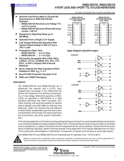
The document describes two 4-port repeaters, the SN65LVDS104 and SN65LVDS105, designed for low-voltage differential signaling (LVDS) applications. The SN65LVDS104 receives differential input levels, while the SN65LVDS105 accepts Low-Voltage TTL (LVTTL) inputs. Both devices are intended for point-to-point baseband data transmission over controlled impedance media such as PCB traces or cables.
| Supply voltage | 3.3 V (nominal) |
|---|---|
| Operating temperature range | -40°C to 85°C |
| Package type | D or PW |
| Propagation delay (SN65LVDS104) | 3.1 ns typical |
| Propagation delay (SN65LVDS105) | 2.2 ns typical |
These repeaters operate from a single 3.3-V supply.
The typical propagation delay time for the SN65LVDS104 is 3.1 ns.