
The IDT72255LA/72265LA are dual port, dual rate, deep programmable FIFOs with ultra low latency and programmable flags, which can be used for a variety of applications.
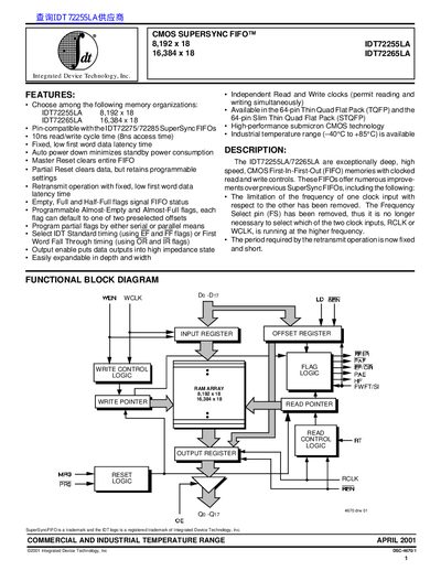
This document describes the IDT72255LA and IDT72265LA, which are exceptionally deep, high-speed CMOS First-In-First-Out (FIFO) memories. These devices offer 8,192 x 18 and 16,384 x 18 memory organizations respectively, utilizing fixed, low first word data latency time and auto power down capabilities to minimize standby consumption.
| Memory Organization IDT72255LA | 8,192 x 18 |
|---|---|
| Memory Organization IDT72265LA | 16,384 x 18 |
| Read/Write Cycle Time | 10ns |
| Technology | CMOS Supersync FIFO |
| Package Types | 64-pin TQFP and 64-pin STQFP |
| Temperature Range | -40°C to +85°C |
The IDT72255LA has an 8,192 x 18 organization and the IDT72265LA has a 16,384 x 18 organization.
Yes, independent Read and Write clocks permit reading and writing simultaneously without frequency restrictions.