
The AT49F004(T) and AT49F4096A(T) are 5-volt, 4-megabit Flash Memories orga- nized as 524,288 words of 8 bits each or 256K words of 16 bits each. Manufactured with Atmel’s advanced nonvolatile CMOS technology, the devices offer access times to 55 ns with power dissipation of just 275 mW. When deselected, the CMOS standby current is less than 300 µA. The device contains a user-enabled “boot block” protection feature. Two versions of the feature are available: the AT49F004/4096A locates the boot block at lowest order addresses (“bottom boot”); the AT49F004T/4096AT locates it at highest order addresses (“top boot”). To allow for simple in-system reprogrammability, the AT49F004(T)/4096A(T) does not require high input voltages for programming. Reading data out of the device is similar to reading from an EPROM; it has standard CE, OE, and WE inputs to avoid bus con- tention. Reprogramming the AT49F004(T)/4096A(T) only requires one pin, CE. For most operations, the other pins are in high-impedance state.
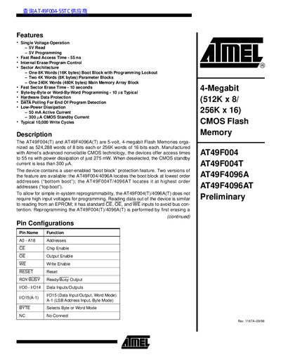
This document is a preliminary datasheet for the Atmel AT49F004(T) and AT49F4096A(T) series of 5-volt, 4-megabit Flash Memories. The devices are organized as 524,288 words of 8 bits each or 256K words of 16 bits each and utilize advanced nonvolatile CMOS technology.
Key features include single voltage operation (5V read and program), fast read access times up to 55 ns, and a sector architecture that separates memory into a boot block, parameter blocks, and a main memory array. The datasheet details pin configurations, block diagrams, device operation modes such as Read, Chip Erase, and Sector Erase, as well as programming sequences for byte-by-byte or word-by-word data entry.
| Capacity | 4-Megabit (512K x 8 / 256K x 16) |
|---|---|
| Read Access Time | 55 ns |
| Active Current | 50 mA |
| Standby Current | 300 uA |
| Write Cycles | 10,000 Write Cycles |
| Erase Time (Chip) | 10 seconds |
The boot block is an 8K words (16K bytes) section.
No, data in the boot block cannot be changed when input levels of 5.5 volts or less are used after lockout is enabled.
The user can override the lockout by applying a 12V + 0.5V signal to the RESET pin during erase or programming operations.