
This document is an introduction to datasheet.
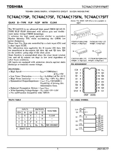
This document is a technical datasheet for the Toshiba TC74AC175P/F/EN/FT series of CMOS digital integrated circuits. The device consists of four D-type flip-flops with a clear input, fabricated using silicon gate and double-layer metal wiring C2MOS technology to achieve high-speed operation similar to Bipolar Schottky TTL while maintaining low power dissipation.
| Max Clock Frequency | 170MHz (typ.) at Vcc = 5V |
|---|---|
| Operating Voltage Range | 2.0~5.5 V |
| Max Power Dissipation (DIP) | 500 mW |
| Operating Temperature Range | -40~85 °C |
| Input Capacitance | 10 pF |
Reset function is accomplished when the clear input is taken low, and all Q outputs are kept in low level regardless of other input conditions.
No, the JEDEC SOP (FN) package is not available in Japan.