
The IDT71V3556 and IDT71V3558 are 3.3V high-speed 4,718,592-bit (4.5 Mega-bit) synchronous SRAMs. They are designed to eliminate dead bus cycles when turning the bus around between reads and writes, or writes and reads. Thus, they have been given the name ZBTTM, or Zero Bus Turnaround. Address and control signals are applied to the SRAM during one clock cycle, and two cycles later the associated data cycle occurs, be it read or write. The IDT71V3556/58 contain data I/O, address and control signal registers. Output enable is the only asynchronous signal and can be used to disable the outputs at any given time. A Clock Enable (CEN) pin allows operation of the IDT71V3556/58 to be suspended as long as necessary. All synchronous inputs are ignored when (CEN) is high and the internal device registers will hold their previous values. There are three chip enable pins (CE1, CE2, CE2) that allow the user to deselect the device when desired. If any one of these three are not asserted when ADV/LD is low, no new memory operation can be initiated. However, any pending data transfers (reads or writes) will be completed. The data bus will tri-state two cycles after chip is deselected or a write is initiated.
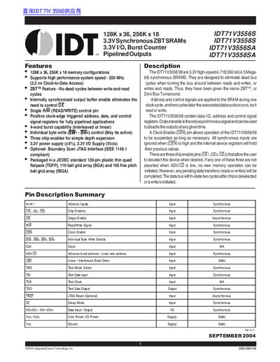
This document describes the IDT71V3556/58 family of 3.3V high-speed synchronous SRAMs available in 128K x 36 and 256K x 18 configurations. The devices utilize a Zero Bus Turnaround (ZBT) feature to eliminate dead cycles between read and write operations, supporting system speeds up to 200 MHz.
| Memory Configurations | 128K x 36, 256K x 18 |
|---|---|
| Maximum System Speed | 200 MHz |
| Clock-to-Data Access Time | 3.2 ns |
| Supply Voltage (VDD) | 3.3V (+/- 5%) |
| Package Types | 100-pin TQFP, 119-ball BGA, 165-ball fBGA |
ZBT stands for Zero Bus Turnaround and eliminates dead cycles between write and read cycles.
The device has three chip enable pins (CE1, CE2, CE3) for simple depth expansion.