
This document describes the features and characteristics of models such as SN54LVTH18512, SN54LVTH182512, SN74LVTH18512, and SN74LVTH182512. These products are 3.3V ABT SCAN test devices with 18-bit universal bus transceivers. They support mixed-mode signal operation, compatible with 5V input and output voltages with 3.3V VCC. They can operate with unregulated battery down to 2.7V. The UBT (Universal Bus Transceiver) combines D-type latches and D-type flip-flops for operation in transparent, latched, or clocked mode. Bus hold on data inputs eliminates the need for external pullup/pulldown resistors. The B-port outputs of 'LVTH182512 devices have equivalent 25-Ω series resistors, so no external resistors are required. They are compatible with the IEEE Std 1149.1-1990 (JTAG) test access port and boundary-scan architecture. The SCOPE instruction set includes the required instructions and optional CLAMP and HIGHZ, supporting parallel-signature analysis at inputs, pseudo-random pattern generation from outputs, sample inputs/toggle outputs, binary count from outputs, device identification, and even-parity opcodes. Package options include 64-pin plastic thin shrink small outline (DGG) and 64-pin ceramic dual flat (HKC) packages using 0.5-mm center-to-center spacings.
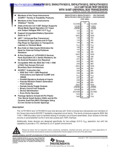
The SN54LVTH18512, SN54LVTH182512, SN74LVTH18512, and SN74LVTH182512 are 3.3-V ABT scan test devices with 18-bit universal bus transceivers designed to support IEEE Std 1149.1-1990 boundary-scan testing of complex circuit-board assemblies. These devices combine D-type latches and D-type flip-flops to allow data flow in transparent, latched, or clocked modes.
The B-port outputs are designed to source or sink up to 12 mA.
These models are characterized for operation over the full military temperature range of —-55°C to 125°C.