
TMS320DM642 is a high-performance digital media processor from Texas Instruments. It has 2-, 1.67-, 1.39-ns instruction cycle time, 500-, 600-, 720-MHz clock rate, eight 32-bit instructions/cycle, 4000, 4800, 5760 MIPS, IEEE 802.3 compliant, fully software-compatible C64x™, 8 independent transmit (TX) channels and 1 receive (RX) channel, eight highly independent functional units, providing a glueless I/F to common video decoder and encoder devices, supports multiple resolutions/video standards, VCXO interpolated control port (VIC), supports audio/video synchronization, host port interface (HPI), 32-bit/66-MHz, 3.3-V peripheral component interconnect (PCI) bus, etc.
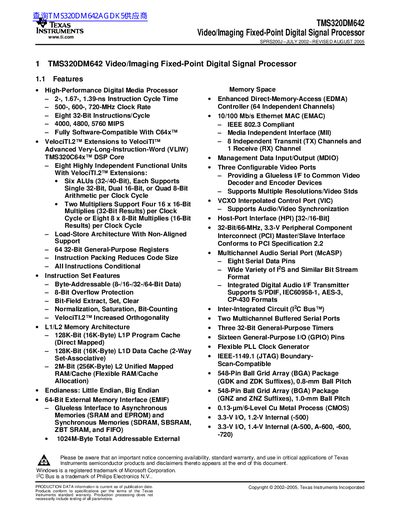
The TMS320DM642 is a Video/Imaging Fixed-Point Digital Signal Processor based on the second-generation VelociTI.2 architecture. It features an advanced Very-Long-Instruction-Word (VLIW) design with eight highly independent functional units, including six ALUs and two multipliers, delivering up to 5760 MIPS at a clock rate of 720 MHz.
The device includes extensive on-chip peripherals such as three configurable video ports supporting multiple resolutions and standards, a 10/100 Mb/s Ethernet MAC, an IEEE-1349.1 (JTAG) boundary-scan interface, and various serial communication ports like McASP and McBSP. It utilizes a two-level cache architecture with L1P and L1D caches and a flexible 2-Mbit Level 2 memory space.
| Instruction Cycle Time | 2-, 1.67-, 1.39-ns |
|---|---|
| Clock Rate | 500-, 600-, 720-MHz |
| MIPS Performance | 4000, 4800, 5760 MIPS |
| Functional Units | Eight Highly Independent Functional Units |
| ALU Support | Single 32-Bit, Dual 16-Bit, or Quad 8-Bit Arithmetic per Clock Cycle |
| Multipliers Support | Four 16 x 16-Bit Multiplies (32-Bit Results) per Clock Cycle |
| L1P Program Cache Size | 128K-Bit (16K-Byte) |
| L1D Data Cache Size | 128K-Bit (16K-Byte) |
| L2 Unified Memory/Cache Size | 2M-Bit (256K-Byte) |
| External Addressable Memory Space | 1024M-Byte |
| Ethernet Speed | 10/100 Mb/s |
| Package Type | 548-Pin Ball Grid Array (BGA) |
The device supports a clock rate up to 720 MHz.
It achieves a performance of up to 5760 million instructions per second.
The L1D Data Cache has a capacity of 128K-Bit.