
This document describes the pin configuration and features of a product in PLCC package. The product conforms to Intel LPC Interface Specification 1.0 and has 8M bits of flash memory for platform code/data storage. It supports automated byte-program and sector-erase operations. The product provides two configurable interfaces: Low Pin Count (LPC) Interface and Address/Address Multiplexed (A/A Mux) Interface. The LPC interface supports a 5-signal communication interface with read and write protection for each sector using software-controlled registers. It also includes general-purpose inputs (GPIs) for platform design flexibility. The A/A Mux interface supports fast on-board or out-of-system programming. The power supply specifications are VCC: 3.3V ± 0.3V and VPP: 3.3V and 12V for fast programming. The product is available in a 40-lead TSOP or 32-lead PLCC package, which is an industry-standard package.
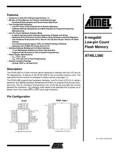
The document describes the Atmel AT49LL080, a nonvolatile Flash memory device designed to interface with the LPC bus for PC applications. It features 8 megabits of storage arranged in sixteen sectors and supports automated byte-program and sector-erase operations.
The device offers two configurable hardware interfaces: Low Pin Count (LPC) for in-system operation at 33 MHz, and Address/Address Multiplexed (A/A Mux) for programming during manufacturing. It operates with a 3.3V supply voltage and supports higher voltages for fast programming.
| Memory Capacity | 8M Bits |
|---|---|
| Operating Voltage (Voc) | 3.3V + 0.3V |
| Programming Voltage (Vpp) | 3.3V and 12V |
| Clock Frequency | 33 MHz |
| Package Types | 40-lead TSOP or 32-lead PLCC |
The device supports Low Pin Count (LPC) for in-system operation and Address/Address Multiplexed (A/A Mux) for programming during manufacturing.
Sector erase and program operations require a Vpp supply of either 3.3V or 12V.
The Low Pin Count (LPC) interface operates at a maximum of 33 MHz.
The high-performance memory core is arranged in sixteen sectors.