
This document describes the performance, characteristics, and functions of SANYO Semiconductor Co., Ltd. products, but does not guarantee their performance, characteristics, and functions when mounted in the customer's products or equipment. The products mentioned in this document are intended for standard applications in general electronic equipment and are not intended for special applications that require extremely high reliability and may directly threaten human lives or cause harm to human bodies.
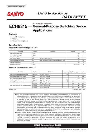
The ECH8315 is a general‑purpose P‑channel silicon MOSFET offered by SANYO Semiconductor. It features low on‑resistance, AV drive capability, and complies with halogen‑free regulations, making it appropriate for a wide range of electronics such as home appliances, AV equipment, and industrial devices.
The datasheet provides absolute maximum ratings, electrical characteristics, and package dimensions. Key parameters include a drain‑to‑source voltage of –30 V, a typical on‑state resistance of 44 mΩ, and a total gate charge of 18 nC. Detailed switching time data and recommended usage notes are also included.
| Drain-to-Source Voltage (V_DSS) | -30 V |
|---|---|
| Gate-to-Source Voltage (V_GS) | +20 V |
| Continuous Drain Current (I_D) | 7.5 A |
| Input Capacitance (C_iss) | 875 pF |
| Total Gate Charge (Q_g) | 18 nC |
The device is rated for a maximum drain‑to‑source voltage of –30 V.
The storage temperature range is –55 °C to +150 °C.
The package dimensions are given in the datasheet under the “Package Dimensions” section (typical 0.65 mm × 0.3 mm for the source pins).