
SY100S839V is a low skew ÷2/4, ÷4/5/6 clock generation chip designed explicitly for low skew clock generation applications.
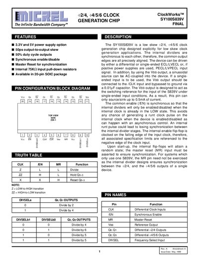
The SY100S839V is a low‑skew +2/4, +4/5/6 clock generation chip offering 3.3 V and 5 V power‑supply options, 50 ps output‑to‑output skew, and 50% duty‑cycle outputs. It supports differential or single‑ended ECL/LVPECL inputs and includes a VBB reference output for single‑ended operation.
The document details pin assignments, truth tables, DC and AC electrical specifications, logic and timing diagrams, and ordering information for the 20‑lead SOIC package. Key performance figures include a 1 GHz maximum toggle frequency and 0.5 mA source/sink capability on the VBB pin.
| Power Supply Options | 3.3 V and 5 V |
|---|---|
| Power Supply Current (IEE) typical | 95 mA |
| Maximum Toggle Frequency (fMAX) | 1000 MHz |
| Duty Cycle | 50 % |
| Input High Current (MH) | 150 µA |
The chip can be powered from either a 3.3 V or a 5 V supply.
The /EN input is synchronous and only enables the internal dividers when the internal clock is already low, preventing runt pulses.