
This is a document of Motorola TMOS Power MOSFET Transistor Device Data. The device is an N-Channel Enhancement-Mode Silicon Gate MOSFET designed to withstand high energy in avalanche and commutation modes. It also features a drain-to-source diode with a fast recovery time, suitable for low voltage, high-speed switching applications in power supplies, converters, and PWM motor controls. The device is particularly well-suited for bridge circuits where diode speed and commutating safe operating areas are critical and offers additional safety margin against unexpected voltage transients.
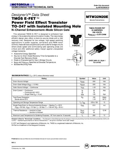
The MTW32N20E is a N‑channel enhancement‑mode silicon‑gate TMOS power MOSFET designed for high‑speed, low‑voltage switching in power supplies, converters, and PWM motor controls. It features a 200 V drain‑source rating, 32 A continuous drain current, and an isolated mounting hole in a TO‑247 package.
Key specifications include a typical R_DS(on) of 0.075 Ω, avalanche energy of 810 mJ, and a maximum power dissipation of 180 W. The datasheet also details dynamic switching characteristics, thermal resistance, and safe operating area curves for reliable design.
| Drain‑Source Voltage (V_DSS) | 200 V |
|---|---|
| Continuous Drain Current (I_D) | 32 A |
| Total Power Dissipation (P_D) | 180 W |
| Junction‑to‑Case Thermal Resistance (RθJC) | 0.7 °C/W |
| Package | TO‑247 with isolated mounting hole |
The device can handle a continuous drain current of 32 A at 25 °C.
The avalanche energy is specified as 810 mJ at a starting junction temperature of 25 °C.
It is supplied in a TO‑247 package with an isolated mounting hole.