
This document describes the features and characteristics of the 1.5V Drive Pch + Pch MOSFET QS8J12 from ROHM, including low on-resistance, small high power package, and low voltage drive.
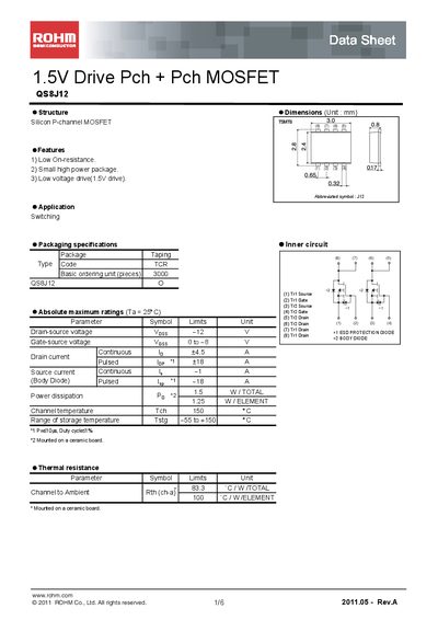
The QS8J12 is a 1.5 V drive P‑channel MOSFET with low on‑resistance and a small high‑power package, intended for switching applications. Key features include low voltage drive (1.5 V), low on‑resistance, and a compact package.
The datasheet lists absolute maximum ratings, thermal resistance, and detailed electrical characteristics such as drain‑source voltage, gate‑source voltage, continuous and pulsed drain currents, on‑state resistance, and power dissipation. Application circuits and measurement setups are also provided.
| Drain‑source voltage (VDS) | -12 V |
|---|---|
| Gate‑source voltage (VGS) | 0 to -8 V |
| Continuous drain current (ID) | +45 A |
| Pulsed drain current (ID,pulse) | +18 A |
| Power dissipation per element | 1.25 W |
| Channel temperature limit (TCH) | 150 °C |
| Storage temperature range | -55 °C to +150 °C |
| On‑state resistance (RDS(on)) typical | 27 mΩ |
| Gate threshold voltage (VTH) | 0.3 V to 1.0 V |
The QS8J12 can withstand a drain‑source voltage of up to -12 V.
It is rated for a continuous drain current of +45 A.
The typical on‑state resistance is 27 mΩ.
The device is designed for a low voltage drive of 1.5 V.