
The document introduces the characteristics of the DS1035 series products, including three independent logic buffered delays and accurate pin descriptions.
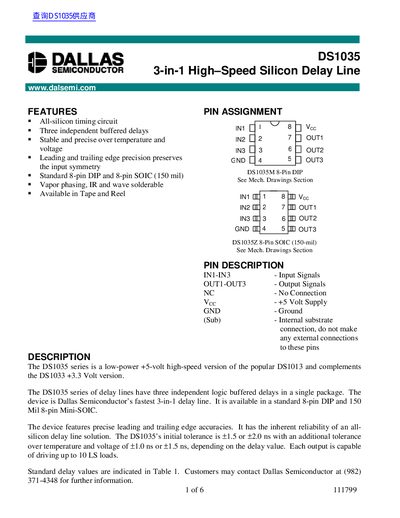
The DS1035 is a low‑power, +5 V, high‑speed silicon delay line offering three independent buffered delays in a single 8‑pin package. It delivers precise leading and trailing edge timing with tolerances as low as ±1.5 ns.
The manual details the device’s features, pin description, logic diagram, delay tables, test setup, absolute maximum ratings, DC and AC electrical characteristics, test conditions, and terminology definitions, enabling engineers to integrate and evaluate the part effectively.
| Supply Voltage (VCC) | 4.75 V – 5.25 V |
|---|---|
| Active Current | 35 mA |
| High Level Input Voltage | 2.2 V |
| Low Level Input Voltage | -0.5 V to 0.8 V |
| High Level Output Current | 1.0 mA |
| Low Level Output Current | 12 mA |
| Operating Temperature | 0 °C to 70 °C |
| Storage Temperature | -55 °C to +125 °C |
| Short‑Circuit Output Current | 50 mA for 1 s |
The DS1035 operates with a supply voltage (VCC) between 4.75 V and 5.25 V.
Absolute maximum ratings include a pin voltage of –1.0 V to +7.0 V, operating temperature 0 °C to 70 °C, storage temperature –55 °C to +125 °C, soldering temperature 260 °C for 10 s, and a short‑circuit output current of 50 mA for 1 s.
The DS1035 provides three independent buffered delays in a single package.
Each output can drive up to 10 LS loads.