
This document describes a 1-bit to 2-bit address driver designed for 2.3V to 3.6V VCC operation. Diodes to VCC have been added on the inputs to clamp overshoot. Active bus-hold circuitry holds unused or undriven inputs at a valid logic state. Use of pullup or pulldown resistors with the bus-hold circuitry is not recommended. The outputs, which are designed to sink up to 12 mA, include series damping resistors to reduce overshoot and undershoot. The ALVCHS162830A is an improved version of the LVCHS162830 (non-A version) and has been optimized for lower power consumption and higher AC drive. Higher AC drive provides capability to drive loads with a faster edge rate. To ensure the high-impedance state during power up or power down, the output-enable (OE) input should be tied to VCC through a pullup resistor; the minimum value of the resistor is determined by the current-sinking capability of the driver.
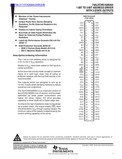
The 74ALVCHS162830A is a 1‑bit to 2‑bit address driver with three‑state outputs, designed for 2.3 V to 3.6 V operation. It includes built‑in series damping resistors, bus‑hold circuitry, and ESD protection, making it suitable for low‑power and high‑speed address‑line applications.
The datasheet details absolute maximum ratings, electrical and switching characteristics, mechanical dimensions, and packaging options (active TSSOP DBB, 80‑pin). It also contains ordering information, availability status, and TI’s standard warranty and disclaimer notices.
| Supply voltage range | -0.5 V to 4.6 V |
|---|---|
| Operating temperature range | -40 °C to 85 °C |
| Package type | TSSOP DBB |
| Pin count | 80 |
The device operates from –0.5 V up to 4.6 V supply voltage.
It is rated for a free‑air operating temperature from –40 °C to 85 °C.
The TSSOP DBB package contains 80 pins.