
CD54HC640 and CD74HC640 are inverting buffers. The direction of data flow (A to B, B to A) is controlled by the DIR input. Outputs are enabled by a low on the Output Enable input (OE); a high OE puts these devices in the high impedance state.
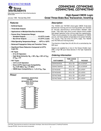
The CD54HC640, CD74HC640, CD54HCT640 and CD74HCT640 are high‑speed CMOS logic devices that provide octal three‑state bus transceiver functionality with inverting operation. They feature buffered inputs, three‑state outputs, and are suitable for multiple‑data‑bus architectures, offering low power dissipation and the ability to drive up to 15 LSTTL loads.
The datasheet includes detailed pinouts for CERDIP, PDIP and SOIC packages, absolute maximum ratings, DC electrical specifications, switching performance, test circuits, packaging options, mechanical dimensions, and legal notices. Ordering information lists part numbers, temperature ranges, and package types for each device variant.
| Operating Temperature Range | -55°C to 125°C |
|---|---|
| Supply Voltage Range (HC Types) | 2 V to 6 V |
| Supply Voltage Range (HCT Types) | 4.5 V to 5.5 V |
The direction of data flow (A to B or B to A) is controlled by the DIR input.
Outputs are enabled when the Output Enable (OE) input is low; a high OE puts the device in high‑impedance mode.
These devices are sensitive to electrostatic discharge; proper ESD handling procedures should be followed.