
The CDCF2510 is a high-performance, low-skew, low-jitter, phase-lock loop (PLL) clock driver from Texas Instruments. It uses a PLL to precisely align, in both frequency and phase, the feedback (FBOUT) output to the clock (CLK) input signal. It is specifically designed for use with synchronous DRAMs. The CDCF2510 operates at 3.3V VCC. It also provides integrated series-damping resistors that make it ideal for driving point-to-point loads. One bank of ten outputs provide ten low-skew, low-jitter copies of CLK. Output signal duty cycles are adjusted to 50%, independent of the duty cycle at CLK. The outputs can be enabled/disabled with the control (G) input. When the G input is high, the outputs switch in phase.
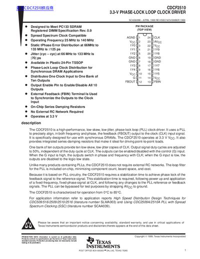
The CDCF2510 is a high‑performance, low‑skew, low‑jitter phase‑lock loop clock driver designed for 3.3 V operation. It distributes a single clock input to ten synchronized outputs, each with integrated series‑damping resistors and 50 % duty cycle.
The device operates from 25 MHz to 140 MHz, requires no external RC network, and includes on‑chip loop filtering. It is qualified for temperatures from 0 °C to 85 °C and includes specifications for supply voltage, output current, phase error, and jitter.
| Operating frequency | 25 MHz to 140 MHz |
|---|---|
| Operating temperature range | 0 °C to 85 °C |
| High‑level output current | ‑12 mA |
No external RC network is required; the loop filter is integrated on‑chip.