
This document is the product manual of IDT71V2556/58 3.3V high-speed synchronous SRAM devices. It introduces the features and characteristics of the devices, including 128K x 36, 256K x 18 memory configurations, 200 MHz high performance system clock speed, ZBTTM feature, single R/W control pin, 4-word burst capability, individual byte write control, three chip enables, 3.3V power supply, 2.5V I/O supply, JEDEC standard 100-pin plastic thin quad flatpack (TQFP), 119 ball grid array (BGA) and 165 fine pitch ball grid array (fBGA).
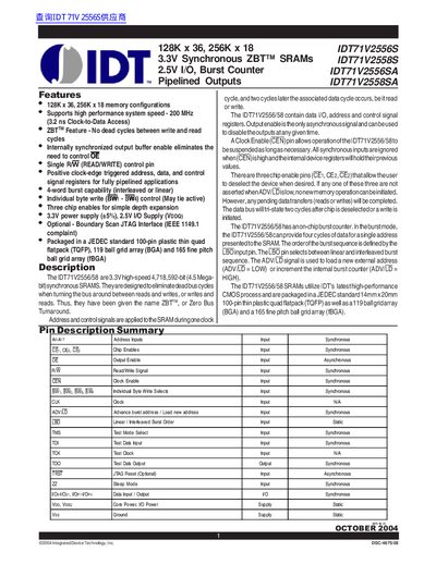
This datasheet describes the IDT71V2556/58 family of synchronous ZBT SRAMs available in 128 K×36 and 256 K×18 configurations. The devices operate at 3.3 V core voltage with 2.5 V I/O, feature a four‑word burst capability, pipelined outputs, and an optional JTAG boundary‑scan interface.
The SRAMs are offered in JEDEC standard 100‑pin thin‑quad flat‑pack (TQFP), 119‑ball BGA, and 165‑fine‑pitch BGA packages. Electrical specifications include a maximum clock frequency of 200 MHz, core supply voltage range 3.135‑3.465 V, I/O supply 2.375‑2.625 V, and temperature ranges of 0 °C to +70 °C (commercial) and –40 °C to +85 °C (industrial).
| Memory capacity | 128 K×36 or 256 K×18 bits |
|---|---|
| Core supply voltage (VDD) | 3.135 V min – 3.465 V max |
| I/O supply voltage (VDDIO) | 2.375 V min – 2.625 V max |
| Maximum clock frequency | 200 MHz (3.2 ns Clock‑to‑Data Access) |
| Operating temperature (commercial) | 0 °C to +70 °C |
| Operating temperature (industrial) | -40 °C to +85 °C |
| Package options | 100‑pin TQFP, 119‑ball BGA, 165‑fine‑pitch BGA |
| Burst capability | 4‑word burst (interleaved or linear) |
The core supply voltage (VDD) ranges from 3.135 V minimum to 3.465 V maximum.
They support a commercial range of 0 °C to +70 °C and an industrial range of –40 °C to +85 °C.
The devices are offered in 128 K × 36‑bit or 256 K × 18‑bit configurations.
They are available in 100‑pin TQFP, 119‑ball BGA, and 165‑fine‑pitch BGA packages.