
This document describes the features and characteristics of the SPRS078F model product, including an advanced multibus architecture with three separate 16-bit data memory buses and one program memory bus, as well as a 40-bit arithmetic logic unit (ALU) and two independent 40-bit accumulators.
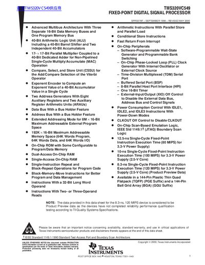
The TMS320VC549 is a fixed‑point digital signal processor based on an advanced modified Harvard architecture with separate program and three data memory buses. It features a 40‑bit ALU, a 17 × 17‑bit parallel multiplier, and on‑chip peripherals such as PLL, serial ports, and timers, delivering high‑speed arithmetic operations.
This datasheet contains detailed pin assignments for the 144‑pin TQFP and BGA packages, signal descriptions, electrical characteristics, timing parameters, absolute maximum ratings, and recommended operating conditions, enabling designers to integrate the DSP into their applications.
| ALU width | 40‑bit |
|---|---|
| Maximum addressable memory | 192 K × 16‑bit (64 K words program, 64 K words data, 64 K words I/O) |
| External program space | 8 M × 16‑bit |
| Instruction execution time (80 MIPS) | 12.5 ns single‑cycle |
| Instruction execution time (100 MIPS) | 10 ns single‑cycle |
| Instruction execution time (120 MIPS) | 8.3 ns single‑cycle |
| Package options | 144‑pin TQFP and 144‑pin BGA |
The device supports up to 192 K × 16‑bit memory, divided into 64 K words of program memory, 64 K words of data memory, and 64 K words of I/O memory.
It is offered in a 144‑pin Plastic Thin Quad Flatpack (TQFP) and a 144‑pin Ball Grid Array (BGA) package.
The instruction executes in 12.5 ns per cycle when operating at 80 MIPS with a 3.3‑V supply.
It features three separate 16‑bit data memory buses.