
The ADC12D040 is a dual, low power monolithic CMOS analog-to-digital converter capable of converting analog in- put signals into 12-bit digital words at 40 Megasamples per second (MSPS), minimum. This converter uses a differential, pipeline architecture with digital error correction and an on- chip sample-and-hold circuit to minimize die size and power consumption while providing excellent dynamic perfor- mance. Operating on a single 5V power supply, the ADC12D040 achieves 10.9 effective bits at 10 MHz input and consumes just 600 mW at 40 MSPS, including the reference current. The Power Down feature reduces power consumption to 75 mW. The differential inputs provide a full scale differential input swing equal to 2VREF with the possibility of a single-ended input. Full use of the differential input is recommended for optimum performance. The digital outputs for the two ADCs are available on separate 12-bit buses with an output data format choice of offset binary or 2’s complement. For ease of interface, the digital output driver power pins of the ADC12D040 can be connected to a separate supply voltage in the range of 2.4V to the digital supply voltage, making the outputs compatible with low voltage systems. The ADC12D040’s speed, resolution and single supply op- eration make it well suited for a variety of applications. This device is available in the 64-lead TQFP package.
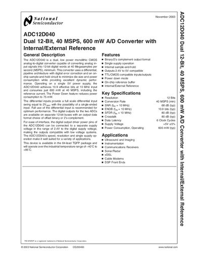
The ADC12D040 is a dual, low‑power CMOS analog‑to‑digital converter that delivers 12‑bit resolution at a minimum conversion rate of 40 MSPS. It operates from a single 5 V supply, offers internal or external reference options, and includes a power‑down mode to reduce consumption.
The document details the device’s pinout, absolute maximum and operating ratings, electrical characteristics, recommended layout practices, and typical applications such as ultrasound imaging, communications receivers, and DSP front ends. Ordering information, physical dimensions, and compliance statements are also included.
| Resolution | 12 Bits (min) |
|---|---|
| Conversion Rate | 40 MSPS (min) |
| Power Consumption (typical) | 600 mW |
| Supply Voltage Range | +4.75 V to +5.25 V |
| Full‑Scale Differential Input | 2 V p‑p |
The maximum clock frequency is 55 MHz (minimum guaranteed 40 MHz).