
The ADC088S052 is a low-power, eight-channel CMOS 8-bit analog-to-digital converter specified for conversion throughput rates of 200 kSPS to 500 kSPS. The converter is based on a successive-approximation register architecture with an internal track-and-hold circuit. It can be configured to accept up to eight input signals at inputs IN0 through IN7. The output serial data is straight binary and is compatible with several standards, such as SPI™, QSPI™, MICROWIRE™, and many common DSP serial interfaces. The ADC088S052 may be operated with independent analog and digital supplies. The analog supply (VA) can range from +2.7V to +5.25V, and the digital supply (VD) can range from +2.7V to VA. Normal power consumption using a +3V or +5V supply is 1.2 mW and 6.5 mW, respectively. The power-down feature reduces the power consumption to 0.03 µW using a +3V supply and 0.15 µW using a +5V supply. The ADC088S052 is packaged in a 16-lead TSSOP package. Operation over the extended industrial temperature range of −40˚C to +105˚C is guaranteed.
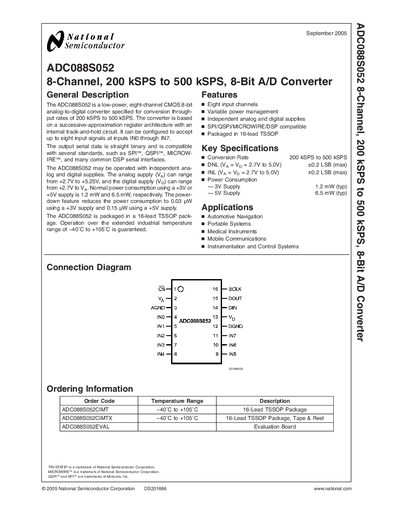
The ADC088S052 is a low‑power, eight‑channel CMOS 8‑bit analog‑to‑digital converter that operates at conversion rates from 200 kSPS up to 500 kSPS. It uses a successive‑approximation register architecture with an internal track‑and‑hold circuit and provides straight‑binary serial output compatible with SPI, QSPI, Microwire and many DSP interfaces.
The device is supplied in a 16‑lead TSSOP package, operates from independent analog and digital supplies (2.7 V to 5.25 V), and includes features such as variable power management, eight input channels, and low‑power operation (as low as 0.03 µW in shutdown). Recommended layout practices include separating analog and digital grounds, short clock traces, and proper decoupling to minimize noise.
| Conversion Rate | 200 kSPS to 500 kSPS |
|---|---|
| Resolution | 8 Bits |
| Analog Supply Voltage | +2.7 V to +5.25 V |
| Differential Non‑Linearity (DNL) | +0.2 LSB (max) |
| Integral Non‑Linearity (INL) | +0.2 LSB (max) |
The ADC088S052 can convert at rates up to 500 kSPS.
Both the analog and digital supplies may be between +2.7 V and +5.25 V.
The device offers eight input channels (INO through IN7).
Yes, the part is lead‑free and RoHS compliant.