
The µPSD3200 Family is a Flash PSD product that combines a Flash PSD architecture with an 8032 microcontroller core. The family features dual banks of Flash memory, SRAM, general purpose I/O and programmable logic, supervisory functions, and access via USB, I2C, ADC, DDC, and PWM channels. It also includes an on-board 8032 microcontroller core with two UARTs, three 16-bit Timer/Counters, and one External Interrupt. Like other Flash PSD families, the µPSD3200 Family supports in-system programming (ISP) via a JTAG ISP interface. The product also includes a large 8KB SRAM, dual bank Flash memories (128KB or 256KB main Flash memory and 32KB secondary Flash memory), and programmable Decode PLD for flexible address mapping of all memories.
The µPSD3200 family combines a Flash PSD architecture with an 8032 microcontroller core, offering dual‑bank Flash, SRAM, programmable logic, and a range of interfaces such as USB, I²C, ADC, DDC and PWM. It supports in‑system programming via JTAG and includes supervisor functions, zero‑power technology, and optional battery‑backed SRAM.
The document provides detailed specifications, pin descriptions for 52‑pin and 80‑pin TQFP packages, functional module diagrams, ordering information, and legal notices. It is intended for designers and engineers evaluating the µPSD3200 devices for embedded applications.
| Main Flash Memory | 128 KByte or 256 KByte |
|---|---|
| Secondary Flash Memory | 32 KByte |
| SRAM | 8 KByte (battery‑back‑up option) |
| Operating Voltage | 4.5 V to 5.5 V (3.0 V to 3.6 V option) |
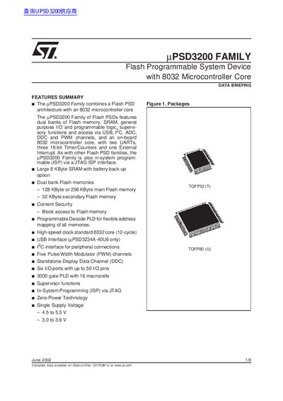
| Package Options | 52‑pin TQFP, 80‑pin TQFP |
| Core Clock Speed | 40 MHz at 5 V, 24 MHz at 3.3 V |
| UARTs | 2 |
| PWM Channels | 5 (four 8‑bit, one 16‑bit) |
The devices support USB, I²C, ADC, DDC, PWM channels, and two UARTs.
Each device includes two UARTs.
Yes, they support in‑system programming via a JTAG ISP interface.
The devices contain an 8 KByte SRAM, with an optional battery‑back‑up feature.