
This document provides preliminary information on a new product that is currently in development or undergoing evaluation. The product is a Flash In-System Programmable (ISP) peripheral designed for 8-bit MCUs with 5V power supply. The main features include dual bank flash memories, concurrent operation of reading and writing, expandable I/O ports, enhanced JTAG serial port, and programmable power management.
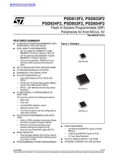
The PSD8XXFX family provides flash‑in‑system programmable (ISP) memory and programmable‑logic (PLD) functionality for 8‑bit MCUs. The devices combine primary and secondary flash, battery‑backed SRAM, and up to 27 configurable I/O ports, enabling flexible embedded designs.
Key features include dual‑bank flash (up to 2 Mbit primary, 256 Kbit secondary), high‑endurance memory (100 k erase/write cycles for flash, 1 k for PLD), low standby current (≈50 µA), and a built‑in JTAG serial port for fast ISP programming.
| Primary Flash Memory | Up to 2 Mbit (8 Uniform Sectors, 32K × 8) |
|---|---|
| Secondary Flash Memory | Up to 256 Kbit (4 Uniform Sectors) |
| Battery‑backed SRAM | Up to 256 Kbit |
| I/O Ports | 27 individually configurable I/O ports |
| Supply Voltage | 5 V ±10 % single supply |
| Standby Current | As low as 50 µA |
| Flash Endurance | 100 000 erase/write cycles |
| PLD Endurance | 1 000 erase/write cycles |
| Data Retention | 15 years |
The device operates from a single 5 V supply with a tolerance of ±10 %.
Each device provides 27 individually configurable I/O ports.
The standby current can be as low as 50 µA.