
TS512 is a high performance dual operational amplifier with frequency and phase compensation built intothe chip.
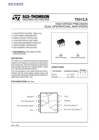
The TS512 is a high‑speed, precision dual operational amplifier featuring low offset voltage, low power consumption, short‑circuit protection and high gain‑bandwidth product. It is intended for professional and telecom applications such as active filters.
The document provides absolute maximum ratings, detailed electrical specifications, pin connections and mechanical dimensions for both DIP‑8 and SO‑8 packages, along with a schematic diagram and macromodel information.
| Supply Voltage (Veo) | +18 V |
|---|---|
| Operating Temperature Range | -40 °C to +125 °C |
| Supply Current | 0.7 mA (min) – 1.2 mA (typ) |
| Input Offset Voltage | 0.5 mV (min) – 2.5 mV (max) |
| Gain‑Bandwidth Product | 1.8 MHz (min) – 3 MHz (typ) |
| Output Short‑Circuit Current | 23 mA |
The device can be powered up to +18 V.
It operates from –40 °C to +125 °C.
Typical supply current is about 1.2 mA.
The gain‑bandwidth product is up to 3 MHz.