
AD5371 is a 40-channel, 14-bit, serial input, voltage output DAC. It has multiple independent output voltage spans, with a maximum output voltage span of 4 times the reference voltage. The product is suitable for applications such as level setting in automatic test equipment, variable optical attenuators, optical switches, industrial control systems, and instrumentation.
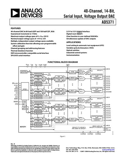
The AD5371 is a 40‑channel, 14‑bit digital‑to‑analog converter offered in 80‑lead LQFP and 100‑ball CSP‑BGA packages. It provides buffered voltage outputs with programmable gain and offset, multiple independent output voltage spans, and a high‑speed serial interface compatible with SPI, QSPI, Microwire, DSP, and LVDS standards.
The document includes a functional block diagram, detailed electrical specifications, timing characteristics for SPI and LVDS interfaces, power‑supply decoupling guidelines, and example schematics for interfacing with DSPs and microcontrollers. Ordering information and package dimensions are also provided.
| Resolution | 14 bits |
|---|---|
| Integral Nonlinearity (INL) | -1 to +1 LSB |
| Differential Nonlinearity (DNL) | -1 to +1 LSB |
| Gain Error | 0.1 % FSR |
| Output Voltage Range | -4 V to +8 V |
| Supply Voltage (DVcc) | 2.5 V to 5.5 V |
| Short‑Circuit Current | 15 mA |
| Power Dissipation (unloaded) | 280 mW |
| Maximum SPI Clock Speed | 50 MHz |
| Number of Channels | 40 |
The AD5371 provides 40 independent DAC channels.
The nominal output voltage range is –4 V to +8 V.
It supports SPI, QSPI, Microwire, DSP‑compatible serial interfaces, and a 100 MHz LVDS interface.
The SPI interface can operate at clock speeds up to 50 MHz.