
The FDB3632 / FDP3632 / FDI3632 / FDH3632 is a 100V, 80A, 9mΩ N-channel PowerTrench® MOSFET from Fairchild Semiconductor. Its features include rDS(ON) = 7.5mΩ (Typ.), Qg(tot) = 84nC (Typ.), low Miller Charge, low QRR body diode, UIS capability (single pulse and repetitive pulse) and AEC Q101 certification. This product can be used for DC/DC converters and off-line UPS, distributed power architectures and VRMs, 24V and 48V systems primary switch, high voltage synchronous rectifier, direct injection/diesel injection systems, 42V automotive load control and electronic valve train systems.
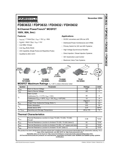
The PowerTrench® N‑Channel MOSFET family provides high current capability (80 A continuous) and low on‑resistance (7.5 mΩ typ.) for applications such as DC/DC converters, off‑line UPS, automotive load control and high‑voltage synchronous rectifiers. The devices are qualified to AEC Q101 and are designed for demanding automotive environments.
Key electrical parameters include a 100 V drain‑to‑source rating, 84 nC total gate charge, and a maximum power dissipation of 310 W. Thermal performance is defined by junction‑to‑ambient resistance values that depend on package type, with detailed models and test circuits provided for design verification.
| Drain to Source Voltage (VDSS) | 100 V |
|---|---|
| On‑Resistance (rDS(on)) | 7.5 mΩ typ. |
| Total Gate Charge (Qg(tot)) | 84 nC typ. |
| Power Dissipation (PD) | 310 W |
| Operating Temperature Range | -55 °C to 175 °C |
| Junction‑to‑Ambient Thermal Resistance (TO‑263) | 43 °C/W |
The typical on‑resistance is 7.5 mΩ when measured at ID = 80 A and VGS = 10 V.
For the TO‑263 package the junction‑to‑ambient thermal resistance is 43 °C/W with a 1 in² copper pad area.