
The DAC108S085 is a full-featured, general purpose OCTAL 10-bit voltage-output digital-to-analog converter (DAC) that can operate from a single +2.7V to +5.5V supply and consumes 1.95 mW at 3V and 4.85 mW at 5V. The DAC108S085 is packaged in a 16-lead LLP package and a 16-lead TSSOP package. The LLP package makes the DAC108S085 the smallest OCTAL DAC in its class. The on-chip output amplifiers allow rail-to-rail output swing and the three wire serial interface operates at clock rates up to 40 MHz over the entire supply voltage range. Competitive devices are limited to 25 MHz clock rates at supply voltages in the 2.7V to 3.6V range. The serial interface is compatible with standard SPI™, QSPI, MICROWIRE and DSP interfaces. The DAC108S085 also offers daisy chain operation where an unlimited number of DAC108S085s can be updated simultaneously using a single serial interface. There are two references for the DAC108S085. One reference input serves channels A through D while the other reference serves channels E through H. Each reference can be set independently between 0.5V and VA, providing the widest possible output dynamic range. The DAC108S085 has a 16-bit input shift register that controls the mode of operation, the power-down condition, and the DAC channels' register/output value. All eight DAC outputs can be updated simultaneously or individually.
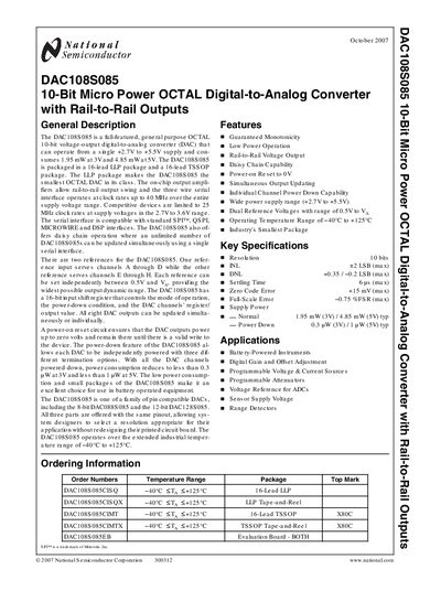
The DAC108S085 is a full‑feature 10‑bit octal digital‑to‑analog converter that operates from a single +2.7 V to +5.5 V supply. It offers rail‑to‑rail output swing, a 40 MHz serial interface compatible with SPI, QSPI, Microwire and DSP, and unlimited daisy‑chain operation.
The device is supplied in 16‑lead LLP and TSSOP packages, supports dual reference voltages (0.5 V to VREF), and operates over an industrial temperature range of –40 °C to +125 °C. Power‑down modes reduce consumption to sub‑pW levels, making it suitable for battery‑powered instruments.
| Resolution | 10 bits |
|---|---|
| Supply Power (3 V) | 1.95 mW typ |
| Supply Power (5 V) | 4.85 mW typ |
| INL (Integral Non‑Linearity) | +2 LSB (max) |
| DNL (Differential Non‑Linearity) | +0.35 / –0.2 LSB (max) |
It operates from a single supply of +2.7 V to +5.5 V.
The device provides eight independent analog output channels (A‑H).
The serial interface can run up to 40 MHz over the full supply range.