
The ADC102S101 is a low-power, two-channel CMOS 10-bit analog-to-digital converter from ADI that supports sample rates up to 1MSPS. The converter is based on a successive-approximation register architecture with an internal track-and-hold circuit. It can be configured to accept one or two input signals, respectively, at inputs IN1 and IN2. The output serial data is straight binary, and is compatible with several standards, such as SPI, QSPI, MICROWIRE, and many common DSP serial interfaces. The ADC102S101 operates with a single supply that can range from +2.7V to +5.25V. Normal power consumption using a +3V or +5V supply is 3.9 mW and 11.4 mW, respec- tively. The power-down feature reduces the power consump- tion to just 0.12 µW using a +3.6V supply, or 0.47 µW using a +5.5V supply. The ADC102S101 is packaged in an 8-lead MSOP package. Operation over the industrial temperature range of −40˚C to +85˚C is guaranteed.
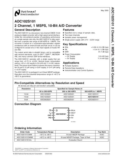
The ADC102S101 is a CMOS 10‑bit ADC that offers two input channels (IN1, IN2) and a high‑speed serial interface compatible with SPI, QSPI, and other DSP standards. It operates from a single supply of 2.7 V to 5.25 V and consumes as little as 0.12 pW in power‑down mode.
Typical applications include portable systems, remote data acquisition, and instrumentation and control. The device is supplied in an 8‑lead MSOP package and is rated for industrial temperature ranges from –40 °C to +85 °C.
| Sample Rate Range | 500 kSPS to 1 MSPS |
|---|---|
| Supply Voltage | +2.7 V to +5.25 V |
| Power Consumption (3 V) | 3.9 mW (typ) |
| Power Consumption (5 V) | 11.4 mW (typ) |
| DNL | +0.26 / –0.16 LSB (typ) |
| INL | +0.4 / –0.1 LSB (typ) |
| Package | 8‑lead MSOP |
| Operating Temperature | -40 °C to +85 °C |
The device operates from a single supply voltage between +2.7 V and +5.25 V.
It provides two analog input channels, labeled IN1 and IN2.
Typical power consumption is 3.9 mW when powered at 3 V.
The ADC can sample up to 1 MSPS.