
The DS90LV028A is a dual CMOS differential line receiver designed for applications requiring ultra low power dissipa- tion, low noise and high data rates. The device is designed to support data rates in excess of 400 Mbps (200 MHz) utilizing Low Voltage Differential Signaling (LVDS) technology. The DS90LV028A accepts low voltage (350 mV typical) dif- ferential input signals and translates them to 3V CMOS output levels. The receiver also supports open, shorted and terminated (100Ω) input fail-safe. The receiver output will be HIGH for all fail-safe conditions.
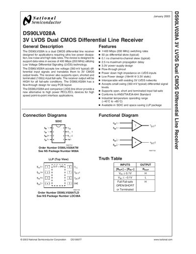
This document describes the DS90LV028A 3V LVDS dual CMOS differential line receiver, including its general description, features, and functional diagrams. It outlines absolute maximum ratings, electrical and switching characteristics, and provides detailed application information such as PCB layout, power decoupling, and termination recommendations.
Additional sections cover fail‑safe operation, probing techniques, cable and connector guidance, pin descriptions, ordering information, typical performance curves, physical dimensions, and a life‑support policy disclaimer. The datasheet is intended for designers and engineers integrating the device into high‑speed LVDS point‑to‑point systems.
| Maximum Data Rate | >400 Mbps (200 MHz) |
|---|---|
| Power Supply Voltage | +3.3 V ±0.3 V |
When inputs are left open, the internal pull‑up/down bias forces the output to a stable HIGH state.