
This document describes an 8-bit flip-flop with 3-state outputs, designed for driving highly capacitive or relatively low-impedance loads. The product is particularly suitable for implementing buffer registers, I/O ports, bidirectional bus drivers, and working registers.
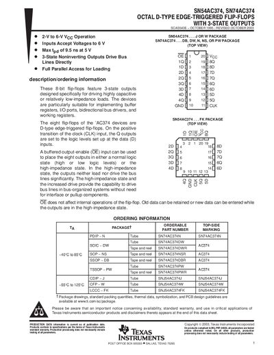
The SN54AC374 and SN74AC374 are 8‑bit, edge‑triggered D‑type flip‑flops with three‑state outputs. They are intended for use as buffers, I/O ports, bidirectional bus drivers, and working registers in bus‑organized systems, allowing high‑impedance states without external pull‑up components.
Key electrical characteristics include a supply voltage range of 2 V to 6 V, propagation delays as low as 9.5 ns at 5 V, continuous output currents up to 50 mA, and maximum clock frequencies up to 100 MHz. The datasheet also lists detailed package information, thermal impedance values, and recommended operating conditions.
| Supply voltage (VCC) | 2 V – 6 V |
|---|---|
| Maximum propagation delay (tpg) | 9.5 ns at 5 V |
| Continuous output current | up to 50 mA |
| Maximum clock frequency | up to 100 MHz |
| Hold time (tH) | 1 ns |
| Package thermal impedance (DB) | 70 °C/W |
The devices operate with a supply voltage (VCC) from 2 V to 6 V.
The maximum clock frequency is up to 100 MHz, depending on the specific package.
The PDIP version of the device has 16 pins.
OE should be tied to VCC through a pull‑up resistor; the minimum resistor value is set by the driver’s current‑sinking capability.