
This data sheet provides detailed information on the SN54LV02A and SN74LV02A dual-input positive NOR gates. These devices operate from 2 to 5.5 V VCC and perform the Boolean function Y = A + B or Y = A•B in positive logic. These devices are fully specified for partial-power-down applications using Ioff. The Ioff circuitry disables the outputs, preventing damaging current backflow through the devices.
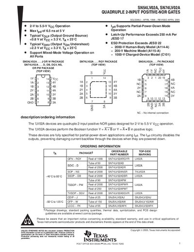
The SN54LV02A and SN74LV02A are quadruple 2‑input positive‑NOR gates designed for operation from 2 V to 5.5 V. They support partial‑power‑down mode and provide typical output characteristics such as low output bounce and ESD protection.
The devices are offered in multiple surface‑mount packages (SOIC, SSOP, TSSOP, QFN, etc.) with standard ordering quantities. Detailed package thermal impedance, storage temperature range, and recommended operating conditions are listed, and additional design data can be found on TI’s website.
| Supply voltage range | 2 V to 5.5 V |
|---|---|
| Input voltage range | 0 V to 5.5 V |
| Output clamp current | -50 mA |
| Package thermal impedance (RGY) | 0.47 °C/W |
They operate from 2 V up to 5.5 V.
Packages include SOIC, SSOP, TSSOP, QFN, and others with various lead counts and thermal characteristics.