
The MAX14820 is an ideal choice for IO-Link® devices and 24V binary sensors/actuators, supporting all specified IO-Link data rates. In IO-Link applications, the transceiver acts as the physical layer interface to a microcontroller running the data-link layer protocol. Additional 24V digital inputs and outputs are provided. Two internal linear regulators generate common sensor and actuator power requirements: 5V and 3.3V. On-board C/Q and DO drivers are independently configurable for push-pull, high-side (PNP), or low-side (NPN) operation. The device detects the IO-Link C/Q wake-up condition and generates a wake-up signal on the active-low WU output. The C/Q and DI inputs have selectable current loads for use in actuators. An SPI™ interface allows configuration and monitoring of the devices. Extensive alarm conditions are detected and communicated through the IRQ output and the SPI inter- face. The devices feature reverse-polarity, short-circuit, and thermal protection. All power lines are monitored for undervoltage conditions. The C/Q driver is specified for sinking/sourcing 300mA. The DO driver is specified for sinking/sourcing 135mA. The device is available in a 4mm x 4mm, 24-pin TQFN package, and is specified over the extended -40NC to +85NC temperature range. Applications include IO-Link sensors, industrial control, and robotics.
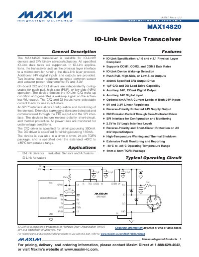
The MAX14820 is an IO‑Link device transceiver that provides a physical‑layer interface for microcontrollers and adds 24 V digital inputs and outputs. It includes two internal linear regulators that generate 5 V and 3.3 V for sensor and actuator power, and configurable push‑pull, high‑side (PNP) or low‑side (NPN) drivers for C/Q and DO signals.
The document lists the device’s absolute‑maximum ratings, DC and AC electrical characteristics, timing diagrams, SPI communication details, protection features (reverse‑polarity, short‑circuit, thermal and undervoltage monitoring), and package information for the 4 mm × 4 mm 24‑pin TQFN. Ordering information and revision history are also provided.
| C/Q Driver Current | ±300 mA |
|---|---|
| DO Driver Current | ±135 mA |
| Operating Temperature Range | -40 °C to +85 °C |
| Package | 4 mm × 4 mm 24‑pin TQFN |
| Maximum SPI Clock Rate | 12 MHz |
The C/Q driver can source or sink up to 300 mA.
The SPI interface supports a maximum clock rate of 12 MHz.
The transceiver includes reverse‑polarity, short‑circuit, thermal protection, and undervoltage monitoring on all power lines.