
This document describes the features and characteristics of the PMWD18UN dual N-channel ultra low level FET, including the use of TrenchMOS™ technology, low threshold, and fast switching.
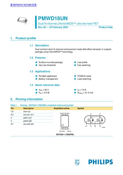
The PMWD18UN is a dual common‑drain N‑channel enhancement mode field‑effect transistor built in a surface‑mounted plastic package using TrenchMOS™ technology. It is intended for portable appliances, PCMCIA cards, battery management and load‑switching applications.
Key specifications include a maximum drain‑source voltage of 30 V, continuous drain current of 7.8 A (peak 32 A), on‑state resistance around 0.21 Ω, total power dissipation of 2.3 W, and an operating temperature range from –55 °C to +150 °C. Pin configuration follows the SOT530‑1 (TSSOP‑8) package.
| Maximum gate‑source voltage (VGS) | 12 V |
|---|---|
| Junction temperature range | -55 °C to +150 °C |
The junction temperature can operate from –55 °C up to +150 °C.