
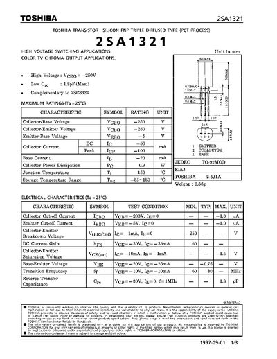
The 2SA1321 is a high‑voltage PNP silicon transistor intended for switching applications such as high‑voltage power supplies and colour‑TV chroma output circuits. The document lists its maximum voltage and current ratings, as well as typical electrical parameters for design use.
Key electrical specifications include collector‑base voltage of 250 V, collector‑emitter voltage of 250 V, and a collector current rating of 50 mA. Power dissipation is limited to 0.9 W, with a junction temperature rating of 150 °C and a storage temperature range of –55 °C to 150 °C. Characteristic curves and safe‑operating‑area graphs are provided to aid designers in selecting appropriate bias conditions.
| Collector‑Base Voltage (VCBO) | 250 V |
|---|---|
| Collector‑Emitter Voltage (VCEO) | 250 V |
| Emitter‑Base Voltage (VEBO) | 5 V |
| Collector Current (IC) | 50 mA |
| Base Current (IB) | 20 mA |
| Power Dissipation (PD) | 0.9 W |
| Junction Temperature (Tj) | 150 °C |
| Storage Temperature Range | -55 °C to 150 °C |
| Input Capacitance (C_R) | 1.8 pF |
The maximum collector‑emitter voltage (VCEO) is 250 V.
The device can be stored between –55 °C and 150 °C.
The transistor is rated for a collector current of 50 mA.
It can dissipate up to 0.9 W of power.