
The AD5303/AD5313/AD5323 is a +2.5 V to +5.5 V, 230μA, dual rail-to-rail voltage output 8-/10-/12-bit DAC. Its features include double-buffered input logic, buffered/unbuffered reference input options, and 0–VREF or 0–2 VREF output range.
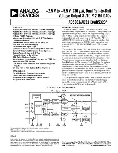
The AD5303/AD5313/AD5323 family provides dual 8‑, 10‑ and 12‑bit buffered DACs in a 16‑lead TSSOP package. They operate from a single +2.5 V to +5.5 V supply, feature rail‑to‑rail output buffers, and support standard SPI, QSPI, Microwire and DSP interfaces.
The document includes full electrical specifications, pin‑out descriptions, ordering guide, mechanical dimensions, and design recommendations such as power‑supply bypassing and grounding. Application notes cover portable battery‑powered instruments, programmable voltage sources, and daisy‑chaining configurations.
| Resolution | 8‑bit (AD5303), 10‑bit (AD5313), 12‑bit (AD5323) |
|---|---|
| Relative Accuracy | +0.15 LSB (AD5303), +0.5 LSB (AD5313), +2 LSB (AD5323) |
| Differential Nonlinearity | +0.02 LSB (AD5303), +0.05 LSB (AD5313), +0.2 LSB (AD5323) |
| Supply Voltage Range | +2.5 V to +5.5 V |
| Power‑Down Current | 200 nA @5 V, 50 nA @3 V |
| Input Current | ≈1 pA |
| Maximum Clock Rate | 30 MHz |
| Package | 16‑Lead Thin Shrink Small Outline Package (TSSOP) |
The devices draw 200 nA at 5 V and 50 nA at 3 V in power‑down mode.
The serial interface supports clock rates up to 30 MHz.
They are supplied in a 16‑lead Thin Shrink Small Outline Package (TSSOP).