
This document is an application note for DD-25664YW-1A OLED display module, including EVK schematic, symbol definition, timing characteristics, connection method and usage method.
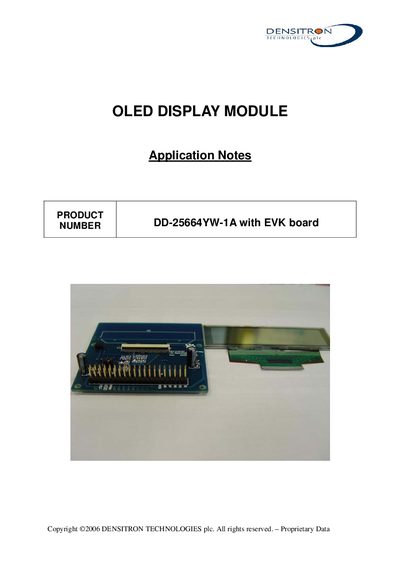
The document describes the DD-25664YW-1A OLED display module and its evaluation (EVK) board. It includes an EVK schematic, symbol definitions for the module pins, detailed timing characteristics for both parallel and MPU 8‑bit interfaces, and wiring diagrams showing the connection between the OLED module and the EVK board.
It also explains how to operate the module, covering reset procedures, recommended initial register settings, and example code snippets for initializing the display, setting scan lines, gray‑scale mode, and other driver functions.
| Address Hold Time (WR) | 10 ns |
|---|---|
| Address Setup Time (WR) | 0 ns |
| System Cycle Time (CS1, CS2) | 200 ns |
| Write Pulse Width (WR) | 60 ns |
| Data Setup Time (DIN[7:0]) | 60 ns |
| Data Hold Time (DIN[7:0]) | 10 ns |
| SD/C Output Delay (SD/COUT) | 30 ns |
| CS Output Delay (CSOUT1, CSOUT2) | 30 ns |
| WR Output Delay (WROUT) | 30 ns |
| DATA Output (DOUT[7:0]) | 30 ns |
Pins DO0‑DO7 are the 8‑bit bi‑directional data bus that connect to the MCU’s data bus.
The chip is enabled when the CS# pin is pulled low.
P/S selects the bus interface: parallel mode when P/S = ‘H’, serial mode when P/S = ‘L’.
Pull the RES pin low to reset the chip, then release it (high) after a short delay.