
This document describes the features and characteristics of the ADP197 charge pump and slew rate control switch, as well as its overtemperature protection function. The document also provides the RDSON values at different temperatures and input voltages, the relationship between VIN and RDSON, and the relationship between load and ground current.
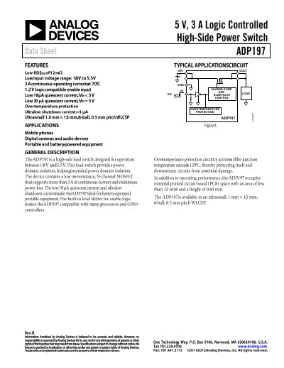
The ADP197 is a charge‑pump and slew‑rate control integrated circuit designed for low‑voltage applications. The datasheet details its electrical parameters such as RDS ON, ground current, and shutdown current across a range of temperatures and load conditions.
Package information, ordering codes, and mechanical dimensions are also provided, showing that the device is offered in a 6‑ball wafer‑level chip‑scale package (WLCSP) suitable for compact board layouts.
| Package Type | 6‑Ball Wafer Level Chip Scale Package (WLCSP) |
|---|---|
| Operating Temperature Range | -40 °C to +85 °C |
| Input Voltage Range | 1.8 V to 5.5 V |
The ADP197 is supplied in a 6‑ball wafer‑level chip‑scale package (WLCSP).
The device operates from –40 °C up to +85 °C.