
This document describes the features and characteristics of the ADP121 CMOS linear regulator. The regulator has a wide input voltage range, adjustable output voltage range, high output current, and low quiescent current. It is suitable for applications such as mobile phones, digital cameras, audio devices, portable and battery-powered equipment.
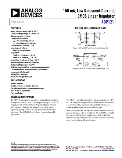
The ADP121 is a CMOS linear regulator that delivers up to 150 mA with very low quiescent current (30 µA typical) and a dropout voltage as low as 90 mV at full load. It features high PSRR (70 dB @1 kHz), low output noise (40 pV rms) and built‑in current‑limit and thermal‑overload protection.
Designed for battery‑powered portable equipment, the device is offered in a 5‑lead TSOT package and a 4‑ball 0.4 mm pitch WLCSP package, both optimized for small board area and stable operation with 1 µF ceramic capacitors.
| Input voltage range | 2.3 V to 5.5 V |
|---|---|
| Output voltage range | 1.2 V to 3.3 V |
| Maximum output current | 150 mA |
| Quiescent current (typical) | 30 µA at 150 mA load |
| Shutdown current | <1 pA |
| Dropout voltage (TSOT, 150 mA) | 90 mV |
| Package options | 5‑lead TSOT, 4‑ball 0.4 mm pitch WLCSP |
| Thermal resistance (TSOT) | 43 °C/W |
| Thermal resistance (WLCSP) | 58 °C/W |
The ADP121 can supply up to 150 mA of output current.
Typical quiescent current is 30 µA when delivering 150 mA.
It is offered in a 5‑lead TSOT package and a 4‑ball 0.4 mm pitch WLCSP package.
The TSOT version has a dropout voltage of 90 mV at 150 mA load.