
ADP198 is a logic controlled, 1A, high-side load switch with reverse current blocking. This data sheet provides detailed information about the product, including features, applications, and typical circuits.
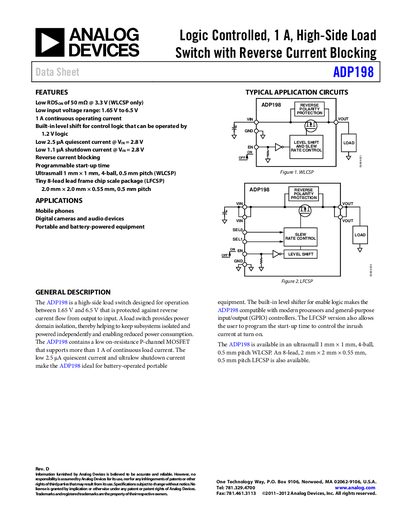
The ADP198 high‑side load switch operates from 1.65 V to 6.5 V and provides reverse‑current protection, making it suitable for battery‑powered portable equipment such as mobile phones and digital cameras. It features a low on‑resistance P‑channel MOSFET, ultra‑low quiescent and shutdown currents, and a built‑in level shifter for 1.2 V logic enable signals.
Two package options are available: an ultra‑small 1 mm × 1 mm 4‑ball WLCSP and an 8‑lead 2 mm × 2 mm × 0.55 mm LFCSP. The device supports programmable turn‑on delay times to control inrush current and includes thermal data for proper board design.
| Input voltage range | 1.65 V to 6.5 V |
|---|---|
| Continuous operating current | 1 A |
| Quiescent current | 2.5 pA |
| Shutdown current | 1.1 pA |
| RDS(on) (typical) | 50 mΩ @ 3.3 V (WLCSP) |
| Package options | WLCSP 1 mm × 1 mm 4‑ball, LFCSP 2 mm × 2 mm × 0.55 mm 8‑lead |
| Maximum continuous drain current | 1000 mA |
| Maximum junction temperature | 125 °C |
The ADP198 operates from 1.65 V up to 6.5 V.
It can supply up to 1 A of continuous load current.
The device is offered in a 1 mm × 1 mm 4‑ball WLCSP and a 2 mm × 2 mm × 0.55 mm 8‑lead LFCSP.
The quiescent current is as low as 2.5 pA at Vin = 2.8 V.